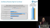
Jan Willis presents the results of this year's Luminaries Survey on future business and technology trends.
|

Katsuya Ueno, GM of AGC Blanks Division, provides an overview of AGC's EUV mask blank business. AGC is the eBeam Initiative's newest member.
|

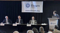
Jim Wiley, Chan-Uk Jeon, and Harry Levinson (pictured left to right) debate the results of this year's Luminaries Survey at the eBeam Initiative annual reception, moderated by Aki Fujimura.
|

Leo Pang of D2S provides his takeaways from Photomask Japan (PMJ), including Best Paper and Best Poster topic PLDC.
|

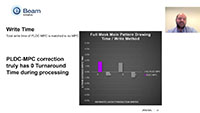
Paris Spinelli of Micron demonstrates in a PMJ Best Paper how PLDC improves mask linearity including variable bias with no increase in turnaround time.
|

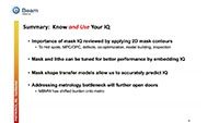
Chris Progler of Photronics explains mask IQ (image quality), including its benefits and potential bottlenecks.
|

Emily Gallagher of imec reprises her keynote from SPIE-AL on climate-aware IC manufacturing.
|

Intel Discusses Large Format Masks for High-NA EUV.
|

IMS Nanofabrication on the Versatility of MBMW Multi-beam Mask Writers.
|

Aki Fujimura of D2S on how PLDC improves uniformity and linearity for all masks.
|

Hiroshi Matsumoto of NuFlare Technology on multi-beam mask writer for High-NA EUV.
|

Aki Fujimura, CEO of D2S, sits down with Jed Rankin of IBM to discuss his leadership of the BACUS Steering Committee and changing the SPIE PUV Conference.
|

Harry Levinson of HJL Lithography summarizes key developments at SPIE-PUV 2024.
|

Glen Scheid of Micron, Harry Levinson of HJL Lithography, and Naoya Hayashi of DNP (pictured left to right) debate the results of the 2024 Luminaries Survey during SPIE PUV with Aki Fujimura as moderator.
Part 1, Part 2
|

Jan Willis presents the results of this year’s Luminaries Survey on future business and technology trends.
|

Toru Fujimori of FUJIFILM Corporation provides an overview on photoresist materials for masks and wafers.
|

Aki Fujimura, CEO of D2S, sits down with Dan Hutcheson of TechInsights for a wide-ranging discussion.
|

We welcome Averroes.ai to the eBeam Initiative.
|

Leo Pang of D2S explains why the mask world is moving to curvilinear mask shapes.
|

Aki Fujimura, co-founder of the eBeam Initiative, celebrates 15 years of eBeam innovation.
|

Matthias Slodowski, Vistec, on extending shaped-beam-lithography.
|

Tom Cecil, Synopsys, on AI-Driven EDA.
|

Jan Willis, Naoya Hayashi, Harry Levinson and David Lam on the eBeam Initiative past and future.
|

Aki Fujimura, CEO of D2S, recaps why manufacturing curvy masks makes curvy design now possible along with key points on the benefits and barriers made by the DAC panel.
|

Glen Scheid of Micron Technology examines the photomask economy in three essential segments: capital equipment, materials, and software.
|

Jan Willis presents the results of this year’s Luminaries Survey on future business and technology trends.
|

Chris Progler from Photronics, Glen Scheid from Micron, and Harry Levinson of HJL Lithography debate the results of the 2023 Luminaries Survey
with Aki Fujimura of D2S as moderator.
|

Matt Hettermann of EUV Tech provides an inside look at the company and its EUV mask metrology.
|

Aki Fujimura of D2S meets up with Donis Flagello of Nikon Research Corporation of America to discuss his career and the “Cambrian explosion” of new technologies.
|

Tom Cecil of Synopsys discusses his extensive career in ILT with Aki Fujimura and how Synopsys is leveraging AI pervasively.
|

Dr. Yu Cao of ASML explains why eBeam inspection and metrology are needed, highlighting new eBeam developments at ASML.
|

Dr. David Lam of Multibeam Corp. describes the misperceptions and opportunities for eBeam lithography.
|

Dr. Harry Levinson of HJL Lithography reflects on developments he observed at SPIE Advanced Litho + Patterning.
|

Aki Fujimura, CEO of D2S, meets with Dr. Frank Abboud of Intel to reflect on key moments from his career.
|

Photomask Japan – eBeam Initiative Update
|

Aki Fujimura puts on his D2S hat to explain the advantages of pixel-based computing with GPU acceleration.
|

Abhishek Shendre of D2S presents the Best Paper awarded at SPIE Photomask 2022.
|

Jan Willis, co-founder of the eBeam Initiative, recaps the results of the 11th annual Luminaries Survey.
|

Ezequiel Russell of Micron makes the case for adopting curvilinear masks for DUV and EUV in advanced memory design.
|

Noriaki Nakayamada of NuFlare Technology explains the advantages of using pixel-level dose correction (PLDC).
|

Aki Fujimura, CEO of D2S, sits down with industry luminary Naoya Hayashi, DNP Fellow, to celebrate his retirement
|

Chris Mack of Fractilia makes the case for a new approach to process window metrology, called Probabilistic Process Window.
|

Jan Willis, co-founder of the eBeam Initiative, interviews Emily Gallagher of imec to discuss her role as BACUS Steering Committee president.
|

Aki Fujimura explains why curvilinear mask shapes are important for both photomask and wafer manufacturers.
|

Aki Fujimura, CEO of D2S, interviews Mike Hermes, vice president of mask technology at Micron, about the changing landscape in mask making, including the shift to multi-beam mask writing and curvilinear masks.
|

Dr. Harry J. Levinson comments on winning the 2022 SPIE Frits Zernike Award and shares his experiences in lithography and what to expect in the future.
|

Leo Pang of D2S provides an overview of the evolution of ILT from his SPIE JM3 ILT review paper published in 2021.
|

Tom Cecil of Synopsys, Mikael Wahlsten of Mycronic, and Chris Progler of Photronics discuss the 2021 eBeam Initiative Luminaries survey.
|

Aki Fujimura, CEO of D2S, interviews Naoya Hayashi of DNP on his impressions of the SPIE Photomask Technology conference.
|

Chris Spence of ASML describes the importance of contour-based mask metrology in modeling advanced masks.
|

Aki Fujimura of D2S interviews Vivek Singh about his new role as VP, Advanced Technology Group at NVIDIA
|

Thomas Cecil of Synopsys explains the benefits of curvilinear ILT mask synthesis.
|

Peter Buck of Siemens Digital Industries Software makes the case for a new standard for curvilinear data.
|

Leo Pang of D2S recaps in Chinese a joint paper with Micron Technology on enabling faster VSB writing of 193i curvilinear ILT masks. Also in English.
|

Aki Fujimura of D2S interviews Harry Levinson of HJL Lithography on his takeaways from the SPIE Advanced Lithography Conference. Leo Pang of D2S offers his perspective on the conference highlights in Chinese.
|

Yuichiro Yamazaki of TASMIT, one of our newest members, explains how NGR massive eBeam metrology and inspection supports cutting-edge wafer processes and applications.
|

Noriaki Nakayamada of NuFlare Technology provides the latest results of writing curvilinear masks with NuFlare’s MBM-2000 multi-beam mask writer, which uses a new data format supporting curvy shapes.
|

Aki Fujimura of D2S hosts a virtual panel discussion about curvilinear masks with industry luminaries Ezequiel Russell of Micron Technology, Noriaki Nakayamada of NuFlare Technology, and Danping Peng of TSMC during SPIE-AL 2021.
|

Dr. Harry Levinson of HJL Lithography shares his impressions of the SPIE Photomask Technology + EUV Lithography Conference; Leo Pang’s impressions in Chinese
|

Aki Fujimura highlights results of the sixth annual eBeam Initiative Mask Makers survey; Jan Willis shares the results of the ninth annual eBeam Initiative Luminaries survey
|

Leo Pang presents the results of a joint paper with Micron Technology on how to enable faster VSB writing of 193i curvilinear ILT masks
|

Ajay Baranwal, director of the Center for Deep Learning in Electronics Manufacturing (CDLe), demonstrates the use of digital twins to create SEM images
|

Leo Pang of D2S reviews a GPU-accelerated approach to curvilinear ILT and how the mask could be written with VSB machines
|

Ezequiel Russell of Micron, the newest member of the eBeam Initiative, answers the questions “Why curvilinear masks? Why now?”
|

Aki Fujimura of D2S with SPIE AL 2020 highlights, including EUV, Deep Learning, curvilinear masks; also in Japanese
|

Thomas Kurian of Mycronic describes his company's new laser-based multi-beam photomask writers as well as his deep learning work at CDLe.
|

Leo Pang of D2S also recaps SPIE-AL 2020 developments in Chinese
|

Dr. Leo Pang of D2S explains the importance of ILT digital twins in today’s growing curvilinear ILT world
|

Ajay Baranwal, Center for Deep Learning in Electronics Manufacturing (CDLe), describes five deep learning recipes for the semiconductor mask making industry
|

Jan Willis recaps key findings from this year’s annual eBeam Initiative Perceptions survey
|

Aki Fujimura, CEO of D2S, provides key takeaways from the recent Photomask Technology Conference; also in Japanese
|

D2S modeling expert Ryan Pearman examines the effects of curvilinear mask data on wafer variability and explains why curvilinear features are needed for EUV lithography.
|

Dr. Harry Levinson of HJL Lithography presents the need for faster computations to deal with the complex physics of leading-edge chip making with EUV lithography
|

Aki Fujimura, CEO of D2S, recaps the hot topics from the Photomask Japan Conference; also in Japanese
|

Leo Pang, Chief Product Officer at D2S, reflects on Photomask Japan in Chinese
|

From the eBeam Initiative luncheon event at SPIE, Yu Cao of ASML explores applications of machine learning in computational lithography
|

Aki Fujimura, CEO of D2S, provides his takeaways from SPIE-AL and an update on the Center for Deep Learning in Electronics Manufacturing (CDLe); also in Japanese
|

Jan Willis sits down with Harry Levinson to talk about his new ventures in lithography as well as what’s driving the increase in computation time for EUV
|

Leo Pang, chief product officer of D2S, describes how GPU-accelerated simulation can enable deep learning for both mask and wafer manufacturing; also in Chinese
|

Jan Willis sits down with Ajay Baranwal, director for the new Center for Deep Learning in Electronics Manufacturing (CDLe)
|

Franklin Kalk of Toppan Photomasks examines the state of photomask manufacturing
|

Aki Fujimura, CEO of D2S, highlights key takeaways from this year’s SPIE Photomask Technology and EUV Lithography Conference; also in Japanese
|

Leo Pang of D2S recaps the conference and survey results in Chinese
|

Mike Green of Photronics on EUV mask patterning
|

Steve Teig from Xperi on Deep Learning
|

Aki Fujimura of D2S on Semiconductor and Photomask Growth; also in Japanese
|

Leo Pang of D2S on Industry Growth in Chinese
|

Aki Fujimura, CEO of D2S, talks about EUV shot noise and other SPIE takeaways; also in Japanese; also in Chinese
|

Hiroshi Matsumoto of NuFlare Technology provides an overview of inline pixel-level dose correction (PLDC) for the NuFlare MBM-1000 multi-beam mask writer
|

Laurent Pain of Leti celebrates 50 years of innovation at Leti and reviews key topics from Leti’s new workshop at SPIE
|

Sergey Babin of aBeam Technologies presents on new developments in CD-SEM metrology
|

Tom Faure of GLOBALFOUNDRIES explains what’s new and different with EUV masks
|

Jed Rankin, co-chair of next year’s SPIE Photomask Technology Symposium, shares his predictions on EUV
|

Aki Fujimura, CEO of D2S, provides his takeaways from the latest eBeam Initiative surveys and more;; also in Japanese
|

Leo Pang, chief product officer of D2S, also recaps these developments in Chinese
|

Ryan Pearman of D2S reviews the challenges of mask modeling in the EUV era in part 2 of a series, part 1 on mask modeling in the multi-beam era can be viewed here
|

Jim Wiley, president of SPIE BACUS, talks about this year’s merger of the EUV Lithography Symposium and the SPIE Photomask Conference as well as his predictions on machine learning
|

Aki Fujimura, CEO of D2S, highlights the company’s latest developments as it celebrates its 10th anniversary, as well as recaps hot topics at Photomask Japan such as deep learning, pixel-level dose correction, and the state of EUV, multi-beam NIL;; also in Japanese
|

Leo Pang, chief product officer of D2S, also recaps these developments in Chinese
|

Tom Cecil of Synopsys discusses the resurgence of inverse lithography technology (ILT), including future opportunities for supporting directed self-assembly (DSA) and EUV
|

Greg McIntyre of imec offers his thoughts on what’s driving up confidence in EUV and the latest on imec’s joint venture with JSR in EUV resist development
|

Aki Fujimura, CEO of D2S, looks back at SPIE-AL and forward to PMJ 2017;; also in Japanese
|

Leo Pang, chief product officer of D2S, also recaps these developments, including CSTIC, in Chinese
|

Dr. David Lam, Chairman of Multibeam Corp., explains how eBeam technology can create the foundation for a more secure connected world
|

eBeam industry luminary Brian Grenon offers an analysis of the results of the eBeam Initiative’s 2016 Mask Maker survey
|

Aki Fujimura, CEO of D2S, highlights several key developments at BACUS 2016;; also in Japanese
|

Leo Pang, chief product officer of D2S, also recaps these developments in Chinese
|

Aki Fujimura shares his viewpoint on how all lithography paths lead to multi-beam mask writing
|

Naoya Hayashi of DNP examines both challenges and progress with nanoimprint lithography (NIL) master templates
|

Aki Fujimura, CEO of D2S, recaps the emerging lithography trends presented at Photomask Japan and the agenda for the upcoming eBeam Initiative Taiwan seminar in June
|

Leo Pang, chief product officer of D2S, also reviews these developments—in Chinese—including highlights of the recent China Semiconductor Technology International Conference
|

Dr. Hiroshi Matsumoto of NuFlare Technology introduces his company’s new multi-beam mask writer, the MBM-1000, along with resolution performance results from an alpha version of the tool
|

Doug Resnick of Canon Nanotechnologies -- one of the eBeam Initiative’s newest members--provides an insider’s look at nanoimprint lithography (NIL)
|

Aki Fujimura, CEO of D2S, recaps the buzz at the eBeam Initiative luncheon at the SPIE Advanced Lithography Conference
|

In a new addition to the Fine Line, Leo Pang, chief product officer of D2S, recaps the SPIE and eBeam Initiative highlights in Chinese
|

Brian Grenon of RAVE and Klaus Edinger of ZEISS join Aki Fujimura in breaking down the results of the latest eBeam Initiative surveys during a luminary panel discussion at the eBeam Initiative reception at BACUS
|

The Fine Line welcomes Markus Waiblinger of new eBeam Initiative member ZEISS, who explains how low-energy eBeam technology represents a paradigm shift in photomask repair and helps enable Moore’s Law
|

Industry luminary Dr. David Lam of Multibeam Corporation provides an update on complementary eBeam lithography (CEBL)
|

Aki Fujimura, CEO of D2S, recaps the breaking news and emerging trends that came out of the recently concluded SPIE Photomask BACUS conference, as well as describes what surprised him most about the results of the eBeam Initiative surveys
|

Shot Talk catches up with Aki Fujimura, CEO of D2S, who shares his takeaways from the recent Photomask Japan conference
|

Noriaki Nakayamada of NuFlare describes ways to conquer resist heating effects in VSB mask writing along with a glimpse into multi-beam mask writing
|

Takayuki Nakamura of Advantest brings mask defects at the 1X node into focus with an overview of new 2D- and 3D-based mask defect verification methodologies
|

Shot Talk catches up with Aki Fujimura, CEO of D2S, who shares his thoughts on the key themes and hot topics at SPIE 2015
|

Colin Harris, COO of PMC-Sierra, shares his perspective on why Moore’s law worked at 16nm and the challenge of repeating that at 10nm
|

Industry luminaries Tom Faure, Bob Pack, Noriaki Nakayamada and Aki Fujimura analyze the mask industry’s responses to the 2014 eBeam Initiative survey
|

Shot Talk catches up with Aki Fujimura, CEO of D2S, who shares his thoughts on the key themes and hot topics at BACUS
|

Bob Pack of GLOBALFOUNDRIES describes a potential flow for integrated mask/lithography signoff verification to address mask hotspots
|

Aki Fujimura explains how context-dependent mask effects require simulation-based MDP;; also in Japanese
|

Kang-Hoon Choi of Fraunhofer CNT explores the capabilities, limitations and requirements of corner rounding correction in mask data
|

Aki Fujimura welcomes Dr. Leo Pang to D2S
|

Dr. David Lam, chairman of Multibeam Corp., “Can eBeam lithography ever get into mainstream manufacturing?”
|

Tony Luo, founder of Maglen and the newest member of the eBeam Initiative, introduces multi-column eBeam inspection
|

Dr. Sergey Babin, founder and president of aBeam Technologies, on charging effects and mask hotspots
|

Mark Sheppard from Advantest describes emerging trends in mask metrology
|

Aki Fujimura from D2S reviews
SPIE and looks ahead at PMJ
|

Aki Fujimura explains the mask hotspots trend;; also in Japanese
|

Naoya Hayashi of DNP looks at mask trends and reports MB-MDP results
|

Aki Fujimura, D2S, Fine Line Winter 2013
|

Hugh Durdan, Xilinx, Fine Line Winter 2013
|

Samsung and D2S, Fine Line Winter 2013
|

Ryan Pearman, D2S, Fine Line Winter 2013
|

Sergey Babin, aBeam Technologies, BACUS 2012
|

Brian Grenon, Advanced Technical Instruments,
BACUS 2012
|

Aki Fujimura, D2S, BACUS 2012
|

Michael Smayling, Tela Innovations, SPIE 2012
|

Ryan Pearman, D2S, SPIE 2012
|

David Lam, Multibeam Corporation, SPIE 2012
|

Aki Fujimura, D2S, SPIE 2012
|

Christian Bϋrgel, AMTC, BACUS 2011
|

Naoya Hayashi, DNP, BACUS 2011
|

Aki Fujimura, D2S, BACUS 2011
|

Gek Soon Chua, GLOBALFOUNDRIES, BACUS 2011
|

Franklin Kalk, Toppan Photomasks, BACUS 2011
|
|
Follow Us On:

|
